Microfluidics: A general overview of microfluidics
Definition of microfluidics
Microfluidics is both the science which studies the behaviour of fluids through micro-channels, and the technology of manufacturing microminiaturized devices containing chambers and tunnels through which fluids flow or are confined.
Microfluidics deal with very small volumes of fluids, down to femtoliters (fL) which is a quadrillionth of a liter. Fluids behave very differently on the micrometric scale than they do in everyday life: these unique features are the key for new scientific experiments and innovations.
The key concept related to microfluidics is to integrate in a simple micro-sized system operations that commonly require a whole laboratory.
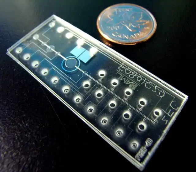
What is a microfluidic chip?
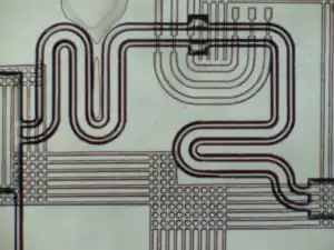
A microfluidic chip is a pattern of microchannels, molded or engraved. This network of microchannels incorporated into the microfluidic chip is linked to the macro-environment by several holes of different dimensions hollowed out through the chip. It is through these pathways that fluids are injected into and evacuated from the microfluidic chip. Fluids are directed, mixed, separated or manipulated to attain multiplexing, automation, and high-throughput systems. The microchannels network design must be precisely elaborated to achieve the desired features (lab-on-a-chip, detection of pathogens, electrophoresis, DNA analysis etc.).
How to control fluids inside microchannels?
To accurately manage fluids inside the microchannels, specific systems are required. These elements can either be found embedded inside the microfluidic chip, such as micropillars, quake valves, tesla valves or outside of it, with flow control systems like syringe pumps, peristaltic pumps or pressure controllers.
Microfluidic devices exploit the physical and chemical properties of liquids and gases at a microscale. Microfluidic devices offer several benefits over conventionally sized systems. Microfluidic devices allow the analysis and use of less volume of samples, chemicals and reagents reducing the global cost of applications. Many operations can be executed at the same time thanks to their compact size, shortening the global time of experiment.
They also offer an excellent data quality and substantial parameter control which allow process automation while preserving the performances. They have the capacity to both process and analyze samples with minor sample handling. The microfluidic chip is elaborated so that the incorporated automation allows the user to generate multi-step reactions requiring a low level of expertise and a lot of functionalities. The microsystems execute functions that extend from detecting toxins to analyzing DNA sequences or creating inkjet printing devices. To learn more about microfluidics applications, visit our dedicated review here.
Today, microfluidics provides efficient tools for multiple research areas, and more specifically for biological analysis:
- Whole biological process integrated and simplified for the end-users
- High-throughput, multiplexed and highly parallelled assays
- Faster analyses due to the shorter reactions and/or separation times
- Portable devices for point-of-care applications
- Low reagent consumptions
- Global cost reduction per analysis
- Accurate measurement, microfluidics allowing to increase the measurement resolution in given applications
What is lab-on-a-chip technology?
A lab-on-a-chip (LOC) is a device performing one or several analyses commonly carried out in a laboratory on a miniaturized scale. It integrates and automates multiple high-resolution laboratory techniques such as synthesis and analysis of chemicals or fluid testing into a system that fits on a chip. There are many advantages to operating at this scale. Samples analysis can occur on location, where the samples are generated, rather than being carried to an extensive laboratory facility. Fluids’ behaviour at this scale makes it easier to control the movement and interaction of samples, causing reactions to be much more potent, and minimizing chemical waste. It also reduces exposure to dangerous chemicals.
Lab-on-a-chip devices are a subdivision of Micro-Electro-Mechanical Systems (MEMS) and often indicated by “Micro Total Analysis Systems” (µTAS). MEMS are data sensors that relay information to a microcontroller which performs the analysis. The composition of these mechanical miniaturized systems depends on the application they are destined to (silicon, glass etc.).
The one encompassing the whole concept is nanofluidics. Nanofluidics examines the behaviour, manipulation, and control of fluids that are limited to structures of nanometric (10-9 m) dimensions. Nanosensors are a primary component of many lab-on-a-chip systems. Sensors have been elaborated using nanomaterials such as carbon nanotubes, suited to apprehend very low volumes like a single cell sample or even smaller samples. These are highly advantageous since they allow a high degree of analytical flexibility in a lab-on-a-chip system while keeping the small size of the device.
What is Organ-on-a-chip technology?
Organ-on-a-chip are 3D cell culture microdevices aiming to reproduce the key functions of living organs on a microfluidic chip. These microfluidic devices are more efficient than conventional cell culture techniques because they are able to mimic microenvironments and reproduce physiological stress. Organ-on-a-chip is a cutting edge technology that enables to perform more accurate research on human physiology and initiate advancements in artificial disease models.
Organs on chips use microfluidics and microfabrication technologies to better replicate the functionalities of living organs. Among them we can find models like gut-on-a-chip, heart on a chip, liver on a chip, lung on a chip, tumor on a chip, muscle on a chip, multiple organs on a chip etc.
Short history of microfluidics
Microfluidics is an integrative domain originating from a mix of microanalysis, biodefence and microelectronics down to the micrometric and sub-micrometric scale. The history of microfluidics started in the 1950’s, with the invention of the first transistor and the apparition of microtechnology. The inkjet printhead technology in which tiny tubes transport the ink for printing was also invented during this period. In the 60’s, computers were miniaturized in order to allow space exploration. The first integrated circuits and microprocessors were created. Technologies like photolithography were developed and allowed to miniaturize and integrate thousands of transistors on semiconductor wafers. These technologies were then used in pressure sensor production.
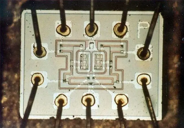
In 1979 was created the first miniaturized gas chromatograph containing mechanical micro-elements integrated on a silicon wafer, thanks to the use of silicon etching procedures developed for the microelectronics industry.
Over the 80s, a new sort of device called Micro Electro Mechanical Systems (MEMS) emerged, allowing industrial applications such as pressure sensors and printheads. By the end of the 1980s, the first microvalves and micro-pumps based on silicon micro-machining were manufactured. During the following years, several silicon-based analysis systems were developed. At this time, microfluidic devices were still made of silicon or glass substrates and required heavy industry facilities and hefty skills.
In the 90s, researchers spent a lot of time investigating the applications of MEMS in biology, chemistry and biomedical fields in order to allow the control of liquids in microchannels. They developed microfluidic fluid handling devices for integrated analysis systems such as micropumps, thermic flow sensors and massic flow sensors and mechanisms for fluid transport, metering, mixing and others.
In the middle 1990s, MEMS technologies implemented tools for genomics research. The military, especially the Defence Advanced Research Projects Agency (DARPA) supported research due to their interest in portable biological and chemical warfare agent detection systems. A leading research area was launched around the elaboration of concepts that could transform the sensor function in a full laboratory analysis on a single microfluidic chip. In the late 90s, the use of soft-lithography allowed the production of cheap microfluidic devices by using polymer molds.
In the early 2000s, technologies based on molding micro-channels in polymers like PDMS encountered a great expansion. A large number of laboratories were able to conduct microfluidic research thanks to the reduction of costs and production time of these devices. Nowadays, a lot of micro-pumps, mixers, microvalves and other devices are available and employed in microfluidic applications.
Microfluidics is now part of scientific innovation in research (space research, biomedical devices, chemical analysis…) and industry (food, cosmetics, oil recovery…). The only limitation is the imagination of its users, and the need to use stable, accurate and responsive equipment for fluid handling. Browse our website to learn more about the most recent research advancements with our research summaries and application notes.
Discover how to choose the right microfluidic flow control system here.
At Elveflow, we are experts in microfluidic instrumentation, we can help you define what system will fit you best.
References
- Nam-Trung Nguyen; Steven Wereley; Seyed Ali Mousavi Shaegh, Fundamentals and Applications of Microfluidics, Third Edition , Artech, 2019
- Sia, S. K., & Whitesides, G. M. (2003). “Microfluidic devices fabricated in Poly(dimethylsiloxane) for biological studies.” Electrophoresis, 24(21), 3563-3576.
- Weibel, D. B., & Whitesides, G. M. (2006). “Applications of microfluidics in chemical biology.” Current Opinion in Chemical Biology, 10(6), 584-591.
- Beebe, D. J., Mensing, G. A., & Walker, G. M. (2002). “Physics and applications of
- microfluidics in biology.” Annual Review of Biomedical Engineering, 4, 261-286.
- Thorsen, T., Maerkl, S. J., & Quake, S. R. (2002). “Microfluidic large-scale integration.” Science, 298(5593), 580-584.
- Unger, M. A., Chou, H. P., Thorsen, T., Scherer, A., & Quake, S. R. (2000). “Monolithic microfabricated valves and pumps by multilayer soft lithography.” Science, 288(5463), 113-116.
For more information or Technical discussion

Microfluidics knowledge
Do you want tips on how to best set up your microfluidic experiment? Do you need inspiration or a different angle to take on your specific problem? Well, we probably have an application note just for you, feel free to check them out!


 Job
Job Collaborations
 Customer
 Other
Other